- 您现在的位置:买卖IC网 > Sheet目录414 > FDB035N10A (Fairchild Semiconductor)MOSFET N-CH 100V 120A D2PAK
�� �
�
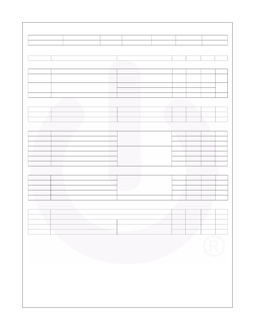
�Package� Marking� and� Ordering� Information�
�Part� Number�
�FDB035N10A�
�Top� Mark�
�FDB035N10A�
�Package�
�D� 2� -PAK�
�Packing� Method�
�Tape� and� Reel�
�Reel� Size�
�330� mm�
�Tape� Width�
�24� mm�
�Quantity�
�800� units�
�Electrical� Characteristics� T� C� =� 25� o� C� unless� otherwise� noted.�
�Symbol�
�Parameter�
�Test� Conditions�
�Min.�
�Typ.�
�Max.�
�Unit�
�Off� Characteristics�
�BV� DSS�
�Drain� to� Source� Breakdown� Voltage�
�I� D� =� 250� μ� A,� V� GS� =� 0� V,� T� C� =� 25� o� C�
�100�
�-�
�-�
�V�
�Δ� BV� DSS�
�/� Δ� T� J�
�I� DSS�
�I� GSS�
�Breakdown� Voltage� Temperature�
�Coefficient�
�Zero� Gate� Voltage� Drain� Current�
�Gate� to� Body� Leakage� Current�
�I� D� =� 250� μ� A,� Referenced� to�
�V� DS� =� 80� V,� V� GS� =� 0� V�
�V� DS� =� 80� V,� T� C� =� 150� o� C�
�V� GS� =� ±20� V,� V� DS� =� 0� V�
�25� o� C�
�-�
�-�
�-�
�-�
�0.07�
�-�
�-�
�-�
�-�
�1�
�500�
�±100�
�V/� o� C�
�μ� A�
�nA�
�On� Characteristics�
�V� GS(th)�
�R� DS(on)�
�g� FS�
�Gate� Threshold� Voltage�
�Static� Drain� to� Source� On� Resistance�
�Forward� Transconductance�
�V� GS� =� V� DS� ,� I� D� =� 250� μ� A�
�V� GS� =� 10� V,� I� D� =� 75� A�
�V� DS� =� 10� V,� I� D� =� 75� A�
�2.0�
�-�
�-�
�-�
�3.0�
�167�
�4.0�
�3.5�
�-�
�V�
�m� Ω�
�S�
�Dynamic� Characteristics�
�C� iss�
�C� oss�
�C� rss�
�Q� g(tot)�
�Q� gs�
�Q� gs2�
�Q� gd�
�Input� Capacitance�
�Output� Capacitance�
�Reverse� Transfer� Capacitance�
�Total� Gate� Charge� at� 10V�
�Gate� to� Source� Gate� Charge�
�Gate� Charge� Threshold� to� Plateau�
�Gate� to� Drain� “Miller”� Charge�
�V� DS� =� 25� V,� V� GS� =� 0� V,�
�f� =� 1� MHz�
�V� DS� =� 80� V,� I� D� =� 75� A,�
�V� GS� =� 10� V�
�(Note� 4)�
�-�
�-�
�-�
�-�
�-�
�-�
�-�
�5485�
�2430�
�210�
�89�
�24�
�8�
�25�
�7295�
�3230�
�-�
�116�
�-�
�-�
�-�
�pF�
�pF�
�pF�
�nC�
�nC�
�nC�
�nC�
�Switching� Characteristics�
�t� d(on)�
�t� r�
�t� d(off)�
�t� f�
�ESR�
�Turn-On� Delay� Time�
�Turn-On� Rise� Time�
�Turn-Off� Delay� Time�
�Turn-Off� Fall� Time�
�Equivalent� Series� Resistance� (G-S)�
�V� DD� =� 50� V,� I� D� =� 75� A,�
�V� GS� =� 10� V,� R� G� =� 4.7� Ω�
�f� =� 1� MHz�
�(Note� 4)�
�-�
�-�
�-�
�-�
�-�
�22�
�54�
�37�
�11�
�1.2�
�54�
�118�
�84�
�32�
�-�
�ns�
�ns�
�ns�
�ns�
�Ω�
�Drain-Source� Diode� Characteristics�
�I� S�
�I� SM�
�Maximum� Continuous� Drain� to� Source� Diode� Forward� Current�
�Maximum� Pulsed� Drain� to� Source� Diode� Forward� Current�
�-�
�-�
�-�
�-�
�214*�
�856�
�A�
�A�
�V� SD�
�t� rr�
�Q� rr�
�Drain� to� Source� Diode� Forward� Voltage�
�Reverse� Recovery� Time�
�Reverse� Recovery� Charge�
�V� GS� =� 0� V,� I� SD� =� 75� A�
�V� GS� =� 0� V,� I� SD� =� 75� A,� V� DD� =� 80� V,�
�dI� F� /dt� =� 100� A/� μ� s�
�-�
�-�
�-�
�-�
�72�
�129�
�1.25�
�-�
�-�
�V�
�ns�
�nC�
�Notes:�
�1.� Repetitive� rating:� pulse-width� limited� by� maximum� junction� temperature.�
�2.� Starting� T� J� =� 25� °� C,� L� =� 1� mH,� I� AS� =� 36.3� A.�
�3.� I� SD� ≤� 75� A,� di/dt� ≤� 200� A/� μ� s,� V� DD� ≤� BV� DSS� ,� starting� T� J� =� 25� °� C.�
�4.� Essentially� independent� of� operating� temperature� typical� characteristics.�
�?2011� Fairchild� Semiconductor� Corporation�
�FDB035N10A� Rev.� C2�
�2�
�www.fairchildsemi.com�
�发布紧急采购,3分钟左右您将得到回复。
相关PDF资料
FDB039N06
MOSFET N-CH 60V 120A D2PAK
FDB045AN08A0_F085
MOSFET N-CH 75V 19A D2PAK
FDB045AN08A0
MOSFET N-CH 75V 90A D2PAK
FDB047N10
MOSFET N-CH 100V 120A D2PAK
FDB075N15A
MOSFET N-CH 150V 130A D2PAK
FDB082N15A
MOSFET N CH 150V 105A D2PAK
FDB088N08
MOSFET N-CH 75V 75A D2PAK
FDB110N15A
MOSFET N-CH 150V 92A D2PAK
相关代理商/技术参数
FDB039N06
功能描述:MOSFET PT3 Low Qg 60V, 3.9Mohm RoHS:否 制造商:STMicroelectronics 晶体管极性:N-Channel 汲极/源极击穿电压:650 V 闸/源击穿电压:25 V 漏极连续电流:130 A 电阻汲极/源极 RDS(导通):0.014 Ohms 配置:Single 最大工作温度: 安装风格:Through Hole 封装 / 箱体:Max247 封装:Tube
FDB039N06_12
制造商:FAIRCHILD 制造商全称:Fairchild Semiconductor 功能描述:N-Channel PowerTrench?? MOSFET 60V, 174A, 3.9m??
FDB045AN08
制造商:FAIRCHILD 制造商全称:Fairchild Semiconductor 功能描述:N-Channel UltraFET Trench MOSFET 75V, 80A, 4.5mз
FDB045AN08_F085
制造商:FAIRCHILD 制造商全称:Fairchild Semiconductor 功能描述:N-Channel PowerTrench?? MOSFET 75V, 80A, 4.5m
FDB045AN08A0
功能描述:MOSFET N-Channel UltraFET
RoHS:否 制造商:STMicroelectronics 晶体管极性:N-Channel 汲极/源极击穿电压:650 V 闸/源击穿电压:25 V 漏极连续电流:130 A 电阻汲极/源极 RDS(导通):0.014 Ohms 配置:Single 最大工作温度: 安装风格:Through Hole 封装 / 箱体:Max247 封装:Tube
FDB045AN08A0
制造商:Fairchild Semiconductor Corporation 功能描述:MOSFET
FDB045AN08A0_06
制造商:FAIRCHILD 制造商全称:Fairchild Semiconductor 功能描述:N-Channel PowerTrench㈢ MOSFET 75V, 80A, 4.5mヘ
FDB045AN08A0_10
制造商:FAIRCHILD 制造商全称:Fairchild Semiconductor 功能描述:N-Channel PowerTrench?? MOSFET 75V, 80A, 4.5m